Research
Semiconductor Quantum Dots
Semiconductor nanoparticles (NP) or nanocrystals (NC) have been investigated for many decades, with particular acceleration in interest upon the discovery of quantum confinement effects thereby yielding quantum dots (QD) from certain well-grown NC. The term NP is commonly used in the case of metal and wide gap semiconductor nanocrystals. The term NC is commonly used in semiconductor nanocrystals, whether covalent II-VI or ionic perovskites, that are colloidally grown. And the term QD applies to select semiconductor nanocrystals for whom their size is on the order of the excitonic Bohr diameter. In the case of colloidal particles on the nm length scale, these terms are often used carelessly and interchangeably. The words have specific meaning in relationship to specific physical effects which give rise to specific key processes that can be measured. Here, we provide a Perspective upon the ways in which size confers function across different families of NP. In this way we aim to find ways to identify their similarities and differences by providing the correct semantics for discussion of the salient processesOur group has done pioneering work on unraveling electron / hole pair (exciton) relaxation dynamics in Semiconductor Quantum Dots as model systems that show quantum size effects as noted below.
Topic 0: Overview of excitonics of Quantum Dots.
The quantum dot, one of the central materials in nanoscience, is a semiconductor crystal with a physical size on the nanometer length scale. It is often called an “artificial atom” because researchers can create nanostructures which yield properties similar to those of real atoms. By virtue of having a size in between molecules and solids, the quantum dot offers a rich palette for exploring new science and developing novel technologies.
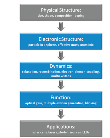
Although the physical structure of quantum dots is well known, a clear understanding of the resultant electronic structure and dynamics has remained elusive. However, because the electronic structure and dynamics of the dot, the “excitonics”, confer its function in devices such as solar cells, lasers, LEDs, and nonclassical photon sources, a more complete understanding of these properties is critical for device development. In this Account, we use colloidal CdSe dots as a test bed upon which to explore four select issues in excitonic processes in quantum dots. We have developed a state-resolved spectroscopic approach which has yielded precise measurements of the electronic structural dynamics of quantum dots and has made inroads toward creating a unified picture of many of the key dynamic processes in these materials.
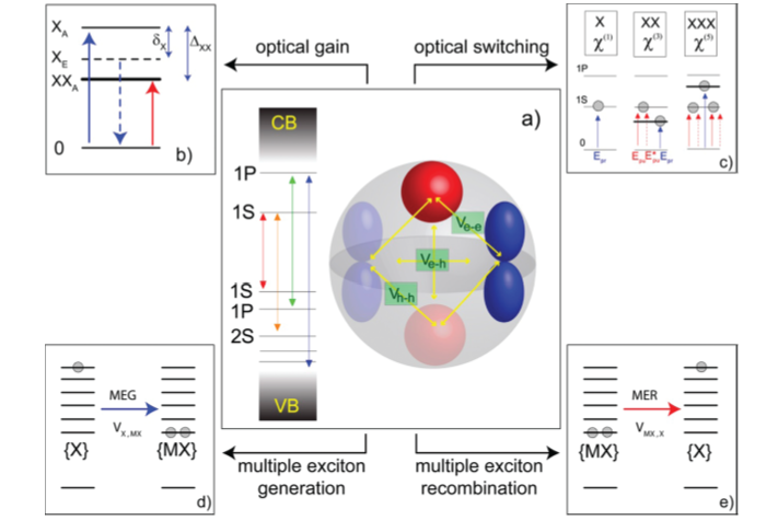
We focus on four main topics of longstanding interest and controversy: (i) hot exciton relaxation dynamics, (ii) multiexcitons, (iii) optical gain, and (iv) exciton−phonon coupling. Using this state-resolved approach, we reconcile long standing controversies related to phenomena such as exciton cooling and exciton−phonon coupling and make surprising new observations related to optical gain and multiexcitons.
Selected publications:
“Unraveling the Structure and Dynamics of Excitons in Semiconductor Quantum Dots”, P. Kambhampati, Acc. Chem. Res. 44, 1 (2011). DOI: 10.1021/ar1000428 - Invited
Topic 1: Multiexcitons in Semiconductor Nanocrystals: A Platform for Optoelectronics at High Carrier Concentration
It is well-known that the shape, size, and composition of semiconductor nanocrystals give rise to a quantized manifold of electronic states, that is, excitons. In addition, these nanocrystals can support multiple excitations per particle under relatively modest conditions. Beyond a laboratory curiosity, these multiexcitons dictate a wide variety of optoelectronic properties of semiconductor nanocrystals including those from lasers, light-emitting diodes, photon sources, and possibly photovoltaics. Whereas their existence has been known for some time, observation of the structure and dynamics of multiexcitons has remained elusive due to their ultrafast lifetimes. In this Perspective, we discuss the first glimpses of the structural dynamics of multiexcitons in CdSe semiconductor nanocrystals as revealed by excitonic state-resolved femtosecond pump/probe spectroscopy. These measurements of multiexciton formation, cooling, and recombination are related to the optical gain performance of nanocrystals. In particular, we show that the gain threshold, bandwidths, and dynamics are dictated by the previously unobserved structural dynamics of multiexcitons.
Selected publications:
“ Multiexcitons in Semiconductor Nanocrystals: A Platform for Optoelectronics at High Carrier Concentration”, P. Kambhampati, J. Phys. Chem. Lett. 3, 1182 (2012). DOI: 10.1021/jz300239j
Topic 2: Hot exciton relaxation dynamics in quantum dots: Radiationless Transitions on the Nanoscale.
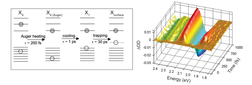
The ability to confine electrons and holes in semiconductor quantum dots (QDs) in the form of excitons creates an electronic structure which is both novel and potentially useful for a variety of applications. Upon optical excitation of the dot, the initial excitonic state may be electronically hot. The relaxation dynamics of this hot exciton is the primary event which controls key processes such as optical gain, hot carrier extraction, and multiple exciton generation. Here, we describe femtosecond state-resolved pump/probe experiments on colloidal CdSe quantum dots that provide the first quantitative measure of excitonic state-to-state transition rates. The measurements and modeling here reveal that there are multiple paths by which hot electrons and hot holes relax. The immediate result is that there is no phonon bottleneck for electrons or holes for excitons in quantum dots. This absence of phonon-based relaxation is confirmed by independent measurements of weak exciton–phonon coupling between the various excitonic states of the dot and the optical and acoustic phonons. We show that the divergence of prior results can be reconciled by adopting this multichannel picture of hot exciton relaxation dynamics. This picture establishes a framework for designing materials with relaxation properties targeted for specific applications. We conclude with connection to hot exciton surface trapping. The process of surface trapping is the key step in creation of the photoproduct which can obscure measurements of optical gain, multiexciton recombination, multiple exciton generation, and single dot blinking. We show that hot exciton surface trapping can effectively compete with hot exciton relaxation, thereby obfuscating these processes.
Selected publications:
“Hot Exciton Relaxation Dynamics in Semiconductor Quantum Dots: Radiationless Transitions on the Nanoscale”, P. Kambhampati, J. Phys. Chem. C 115, 22089 (2011). DOI: 10.1021/jp2058673
Topic 3: Optical Gain and Light Emission in Quantum Dots
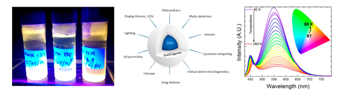
Semiconductor nanocrystals have been extensively studied for optoelectronic applications including light emission, the focus of this review. Historically, the core of the nanocrystal was the main aspect of the system as it gives rise to the confined excitons and multiexcitons which absorb and emit light. In addition to the core, the surface or interface of these nanocrystals is also important by virtue of their small size. Yet, our understanding of the surface is in its early stages in terms of both chemical and electronic structure. Here, we review the ways in which the interface can control the excitonics, which gives rise to optoelectronic function. We focus our discussion on the ways in which the interface can control optical gain for nanocrystal lasers and white light generation for nanocrystal based light emitting diodes. These processes are connected to different interfacial structures. Finally, we discuss two new applications based on surface electronic structure control: optical switching and optical thermometry. The work here suggests that the interface of nanocrystals should be a profitable route for chemical control of the electronic structure which can yield both performance enhancements as well as qualitatively different functional behavior.
Topic 4: On the nature of the Surface of Nanocrystal Quantum Dots
The surface of semiconductor nanocrystals is one of their defining features. The kinetics of surface trapping can be monitored by pump/probe spectroscopy. The thermodynamics of surface trapping is revealed by photoluminescence spectroscopy. We produce the first microscopic picture of how excitons are coupled to the surface. We discuss the possibility of surface excitons in nanocrystals.
The surface of semiconductor nanocrystals is one of their defining features by virtue of their nanometer size. Yet the surface is presently among the most poorly understood aspects of nanocrystal science. This perspective provides an overview of spectroscopic work that has revealed the first insights into the nature of the surface, focusing upon CdSe nanocrystals. We focus on two aspects of surface processes in nanocrystals: the kinetics of surface trapping and the thermodynamics of core/surface equilibria. We describe femtosecond pump/probe spectroscopic experiments which reveal the signatures of carrier trapping at the surface. We also describe temperature dependent steady-state photoluminescence experiments which reveal new aspects of the surface. This work suggest that the surface emission is largely driven by homogeneous broadening via phonon progressions. The implications are that the surface electronic state bears similarity to the quantized excitonic core of the nanocrystal.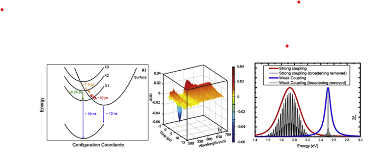
Selected publications:
“On the Kinetics and Thermodynamics of Excitons at the Surface of Semiconductor Nanocrystals: Are There Surface Excitons?”, P. Kambhampati, Chem. Phys. 446, 92 (2015). DOI: 10.1016/j.chemphys.2014.11.008.
Semiconductor Perovskites
The semiconductor perovskite is the current material we focus upon as a model system, in contrast to the CdSe quantum dot nanocrystal which we focused on for the prior era. The perovskite is the newest and most interesting material for our energy future as discussed in the literature. It also supports novel physics of liquid / solid duality, to parallel the discovery of novel physics of quantum confinement effects in quantum dots.
Semiconductor perovskites have rapidly emerged onto the materials science scene since their tremendous initial performance in photovoltaic films in 2014. Since 2016, nanocrystal version of these perovskites (P NC) have become available for easy solution phase synthesis and processing into device architectures. These P NC are also ideal for spectroscopic probing and connecting the basic spectroscopy to the exciton dynamics to the device physics of this emergent class of materials. Unlike the conventional semiconductor quantum dot (QD) which is defined by quantum confined excitons (X). In P NC, the elementary excitation begins in time as a polaron but ends in time as an exciton.
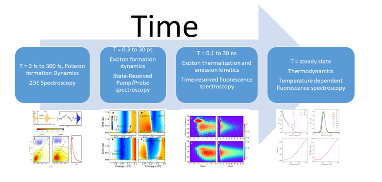
We will for the first time follow the full Life Cycle spanning birth of an excitation from initial polaron formation, to exciton formation, to exciton thermalization, to excitonic emission in perovskite nanocrystals using a suite of three state-of-the-art spectroscopies, made uniquely possible by a one-of-a-kind ultrafast spectroscopy lab. With these three tools of two dimensional electronic spectroscopy (2DE), state-resolved pump/probe (SRPP) spectroscopy, and time-resolved photoluminescence (t-PL) spectroscopy we will monitor all aspects of the dynamical birth, quantum-kinetic evolution, and thermodynamic death of an electronic excitation in a model perovskite system as shown in the Cover Figure below. The impact of this work will be an understanding of structure-function relationships in the newest and most compelling of optoelectronic materials in decades. Our competitive advantage is our world leading ultrafast laser spectroscopy facilities and our prior 15 years expertise in ultrafast exciton dynamics in quantum dots.
Figure: Observing the “product life cycle” of an exciton in a perovskite semiconductor nanocrystal.
Ultrafast Laser Spectroscopy: Method of Investigation which is unique in the world.
The ability to synthesis perovskites, especially perovskite NC, has made it simple to enter the science of semiconducting perovskites for optoelectronic applications. Hence there are many groups doing synthesis and characterization of perovskites and especially P NC due to their ease of synthesis. Making many more materials will not advance our understanding of their novel physical properties and how these properties ultimately give rise to function in optoelectronic devices. What is missing is a set of critical probes of elementary processes that will give rise to broad insight into function. Here we employ a unique in the world, broad based approach focusing on not merely one, but three state-of-the-art spectroscopies. Only this suite of spectroscopies can capture the full distribution of timescales of excitonic processes.
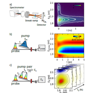
Figure:Schematic illustration of the three time resolved spectroscopies employed here in order of increasing time resolution. a, t-PL is established with a streak camera. b, SRPP is established with a narrow pump pulse and a broadband probe. c, 2DE is established with a phase coherent pump pair and a probe pulse. .
Two-Dimensional Electronic Spectroscopy
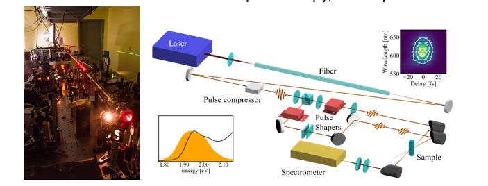
2DES is presently the most sophisticated and information rich form of electronic spectroscopy. The idea is that an electronic system is probed as a function of time like in other time-resolved spectroscopies, but now with a time resolution of 10 fs instead of 100 fs for conventional ultrafast pump/probe spectroscopy. The key point is that two-dimensional spectra are obtained in which one can monitor both excitation and emission of light, with this 10 fs time resolution. Hence once has 2D energy resolution and a new benchmark in time resolution. Finally, by virtue of being coherent, one can measure electronic coherences which can be a sensitive probe of disorder20. Our 2DE Spectrometer was custom designed by us and several optics vendors to represent the world’s state-of-the-art in ultrafast electronic spectroscopy, developed from 2015 to 2017.
Figure :Schematic illustration our custom built, world leading 2DE spectrometer .
State-Resolved Pump/Probe Spectroscopy.
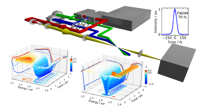
Pump/probe spectroscopy or transient absorption (TA) is a classic one-dimensional time-resolved spectroscopy. The time resolution comes from the time duration of the pump and probe pulses which are typically 100 fs and the 1D energy resolution comes from a spectrally broad probe pulse. In our pump/probe spectrometer developed from 2005 to 2007 we made a far more sophisticated setup than any other in the world, Fig5. Our trick was to be able to synchronize two different pump wavelengths so as to perform two spectrally resolved pump/probe experiments simultaneously. This unique ability enables us to perform exquisitely detailed comparison of dynamics based upon the initial excitonic state. These methods have proven invaluable to unraveling the fundamental excitonics of II-VI NC QD from 2006 to 2012. The key difference of our SRPP from the state of the field using TA is that TA yield 100 fs estimates of carrier thermalization, in contrast SRPP yields 10 fs precision measures of excitonic dynamics
Figure :Schematic illustration our custom built, world leading SRPP spectrometer.
Time-resolved photoluminescence.
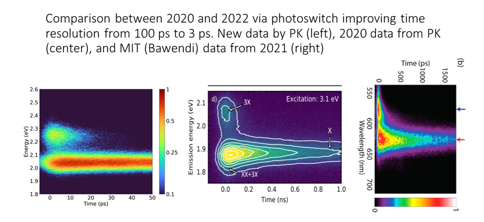
The simplest and most intuitive way to spectroscopically characterize optoelectronic materials is time resolved photoluminescence (t-PL) measurements. Here, one simply sees directly the light emission with some time resolution determined by commercial detectors. These detectors have time resolutions of 1 to 10 ns typically with one dimensional energy resolution produced by a spectrometer. In our case we have a high-end streak camera detector for which we have established 100 ps time resolution, consistent with the state-of-the-art for the mature methods of t-PL. Our t-PL spectrometer will be improved in this proposal to < 5 ps time resolution thereby offering a remarkably powerful, yet simple window into one of the most exciting new classes of system to emerge in materials science in decades.